Tingbo He, head of semiconductor research at Huawei Technologies, published a new academic paper on Thursday addressing concerns about heat dissipation in 3D-stacked chips, marking the company’s third paper on its “τ-law” chip design philosophy in less than four months.
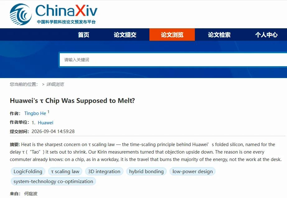
The latest paper, titled “Huawei’s τ Chip Was Supposed to Melt?”, responds to scepticism that folding circuits into three dimensions would inevitably lead to higher power density and thermal issues.
“Heat is the most troublesome hidden concern of the τ-law,” She wrote. “Inside the chip, the main energy consumption does not come from computation itself, but from data transfer.”
Contrary to expectations that circuit folding would dramatically increase transistor density and power density, the paper argues that folding actually reduces energy consumption by shortening critical interconnects. Typical core wire lengths are reduced by 20%, critical path wires by 70%, and the number of clock buffers – among the most power-hungry components – is cut by half, She said.
The additional transistors made possible by circuit folding can be used to build more parallel cores, allowing each core to operate at lower voltage and clock frequency, providing greater flexibility, according to the paper.
“Reduced power consumption in the Kirin chipset does not come from doing less computation, but from less data transfer,” She wrote.
Test results cited in the paper show that compared with the Kirin 9030 Pro, the Kirin 2026 achieves lower frequency, voltage and power density across its NPU, GPU, CPU P-core and DSP modules at equivalent performance levels, while delivering significantly improved performance at full speed. Transistor density increased 55% from approximately 155 million to 238 million per square millimetre. At the same performance level, NPU power consumption fell 66%, GPU dropped 58%, and CPU performance cores decreased 41%. The NPU was particularly notable: maintaining 29 TOPS of computing power, frequency dropped 63%, voltage fell from 0.85V to 0.55V, and power density declined 73%.
For localised hotspots, Huawei’s approach involves two strategies: first, reducing source power density through folding to prevent localised high temperatures; second, proactively designing thermal layouts that place the most heat-intensive modules in the best-cooled positions.
However, She emphasised that folding is not a universal solution but requires iterative system engineering. She noted that the τ-law is a law of time scaling, not energy scaling – if designers use all the time saved to increase frequency, chips could actually become more power-hungry.
Significant engineering challenges remain, including hybrid bonding pitch, wafer warpage, alignment accuracy and EDA tool adaptation, requiring three to five years of sustained effort, She said. While thermal issues have been alleviated by reduced overall power consumption, heat conduction from lower layers remains an unresolved issue.
Huawei previously published the V1 version of the τ-law paper on May 25 and the V2 version on July 4. The τ-law, named after the Greek letter τ (tau) used in physics to denote time constants, represents Huawei’s design philosophy for time-aware chip architecture, according to the company.


 AGIBOT
 Figure AI
 UBTECH